


 EN
·
EN
·  DE
DESemiconductor & Advanced Packaging
As devices shrink and stack, more of the hard steps move to the laser, from wafer dicing and TGV drilling through to the annealing and lift-off steps behind every OLED display. And once a step turns optical, the beam becomes the tolerance: depth, topography and fluence spread eat the process window before the first pulse even fires. That’s the problem we build optics for.
The process moved into the optics, and now the beam is the tolerance
For most of the industry’s history the hard steps were mechanical, and mechanical was forgiving. A diamond blade cutting a 300 µm-plus wafer sets its geometry from the blade, not from an optical process window. Focus drift simply isn’t a failure mode. But the substrate kept changing underneath the tooling. For example, HBM4 puts 12- and 16-high DRAM stacks under a 775 µm package height, driving die to roughly 30–50 µm, where the abrasive force that used to be harmless becomes the dominant source of chipping and die-strength loss. So the hard steps went optical: ablation and stealth dicing remove or cleave the wafer with no mechanical load, ultrafast drilling plus wet etch opens TGV/TSV, and the whole thing scales to panel format for glass-core substrates.
That move buys a lot, and hands the tolerance to the beam. A Gaussian holds its fluence only within its Rayleigh range, so wafer bow, total thickness variation, chuck flatness and via depth now eat the process window directly. Via straightness stops being a power setting and becomes an etch-selectivity problem set by how uniformly the modified zone was written through the full depth. And the same physics governs the display side, where the process is the beam profile: excimer line-beam annealing turns amorphous silicon into the LTPS backbone of every OLED panel, and OLED/µLED lift-off releases millions of emitters at once; in both, grain and release uniformity, and therefore pixel-to-pixel brightness and yield, are set by how flat the fluence is across the field.
All of these are one problem wearing different clothes: hold spot size, taper and fluence stable across the depth and topography the part actually presents. That’s a beam-shape problem, and it’s the one we solve: our 3D line-up delivers extended depth of focus, flat-top and ring/core profiles as passive, high-LIDT optics, each dimensioned to the wafer, substrate or panel spec in front of it.
- Focus over real topography — wafer bow, TTV and chuck flatness, not a nominal flat plane; a Gaussian’s fluence only holds within its Rayleigh range
- Taper through the full depth — via straightness is set by how uniformly the modified zone is written top to bottom, not by pulse energy
- Fluence uniformity across the field — annealing, lift-off and thin-film scribing live or die on a flat profile, where pixel brightness and release yield are decided
Stay in focus, not just in spec
Depth of focus beyond the plane
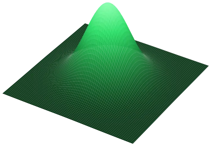
3D Gaussian holds a stable, near-diffraction-limited spot beyond the conventional focal plane: 60–500% more usable depth, depending on shaping type.
A flat-top that doesn't taper
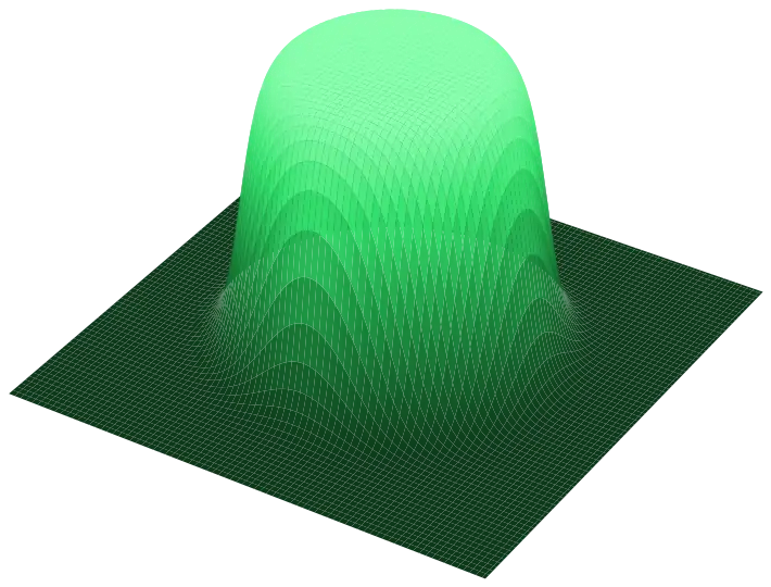
3D Top-Hat holds its size and shape across a multi-millimetre focus range, already proven in production on semiconductor lines.
A ring where you need one
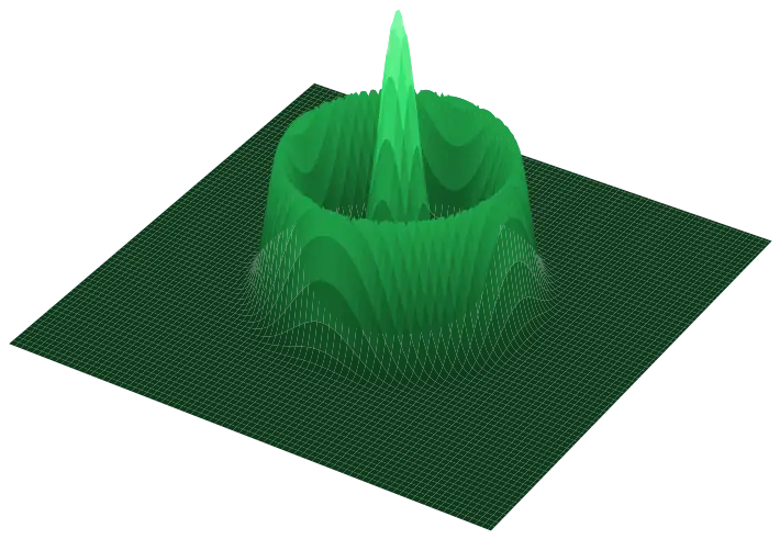
3D Ring-Core concentrates energy at a feature’s perimeter and stays stable off the focal plane, suited to controlled-taper via drilling.
The semiconductor & advanced packaging landscape, and where beam shape is the lever
Semiconductor, advanced packaging and display manufacturing span a wide range of laser processes, but they share one physics problem: hold focus, taper and fluence through the depth and topography of the wafer, substrate or panel. Below is the landscape as we see it, and for a growing number of these we help customers find and build the beam shape that fits.
Wafer dicing (laser ablation)
Ablates the street optically, so no abrasive load reaches the die (the reason it displaced blade dicing on thin and brittle stacks). The cost is a heat-affected zone on the order of 15 µm and debris, both of which scale with how far the fluence drifts off nominal.
Stealth dicing
An IR wavelength the silicon transmits is focused inside the wafer; absorption is confined to the focal volume because it only becomes significant at the intensity reached there. The subsurface modified layer is then cleaved by tape expansion: a dry process with essentially no kerf loss.
Laser grooving
A laser removes the low-k dielectric and metal test structures in the street before a blade completes the cut: the standard hybrid route for BEOL stacks that crack under a blade alone.
TGV / TSV via drilling
Ultrafast pulses write a modified zone through the substrate; a selective wet etch then opens it into a via. Via straightness is governed by etch selectivity (reported at roughly 2.3–4.2 on borosilicate), which depends on how uniformly the modified zone was written along the full depth. Beam geometry, not pulse energy, is the controlling variable.
Wafer thinning
Backgrinding to the 30–50 µm range required for 12- and 16-high HBM stacks. Grinding introduces dislocations and stacking faults that measurably reduce fracture strength, which is why a polish step and a low-stress singulation route are chosen together, not separately.
Laser lift-off (LLO)
A UV pulse absorbed at the interface decomposes a sacrificial layer and releases the device layer from its growth substrate. Because the release either happens or doesn’t at a given fluence, the process is limited by fluence uniformity across the field, not by average power.
Laser debonding
Releases a temporarily bonded carrier after thin-wafer handling with no mechanical stress on the die. Same constraint as LLO: a flat, repeatable fluence distribution over the full irradiated field.
Excimer laser annealing (ELA)
A line-beam UV pulse crystallises amorphous silicon into low-temperature polysilicon (LTPS) for the TFT backplane behind OLED and high-resolution LCD panels. Grain uniformity (and therefore pixel-to-pixel brightness) is set by how flat the fluence is along the line, which is why the line-beam profile is the process.
Laser lift-off for displays (µLED / OLED)
A UV pulse releases OLED or micro-LED device layers from a carrier or growth substrate for transfer onto the panel. Yield across millions of emitters depends on the release happening identically everywhere, so the governing spec is fluence uniformity across the field, not peak energy.
Thin-film patterning (P1/P2/P3)
Selective scribing of stacked electrode, semiconductor and contact layers: the display and thin-film-PV analogue of grooving. Each scribe has to clear its own layer without touching the one beneath, so the process window is a fluence band that a flat profile keeps the whole spot inside.
Laser-induced forward transfer (LIFT) & repair
A focused pulse transfers or ablates material to place, trim or repair individual pixels and traces on a finished panel. It is single-feature work where spot shape and depth stability decide whether the repair matches its neighbours.
Beam profiles for wafer & via processing
3D Top-Hat Beam Shapers
Holds a uniform flat-top across the depth of focus, not just in the focal plane.
Explore → EDOF · focus extension3D Gaussian Focal Shaper
Extends depth of focus up to 5×, so the process stops depending on a knife-edge focus.
Explore → EDOF · ring profile3D Ring-Core Shaper
A ring around a core, stable across the full depth of focus: calmer keyhole, less spatter.
Explore →Not sure which fits? The fit-check on each product page shows the parameters we design against.
Related use cases
Semiconductor processing
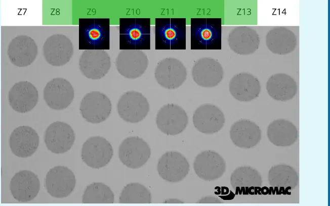
A homogenized flat-top that stays on-size across a 4–6 mm focus range.
Read use case →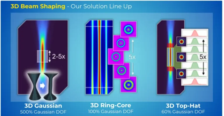
Through-Glass Vias for AI packaging
Why 3D beam shaping is the optics-ready foundation for TGV drilling.
Read white paper →Bring us your process window.
If focus tolerance, taper, or throughput is capping your current laser process, tell us your wafer or substrate spec. We’ll assess feasibility and design the right beam shape together.
Discuss your challenge